Integration with diverse functionalities technology
|
|---|
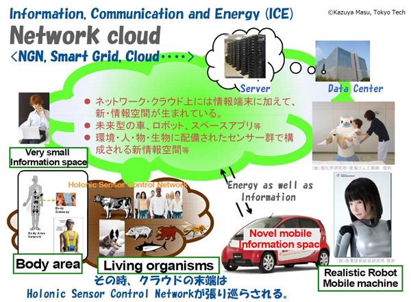 Our life depends on infrastructure network such as electricity, gas, and water, which then developed into communication network such as the internet, land phones and mobile phones to make us live comfortably in a secure and convenient life. In “Network Cloud”, it shows how we run our daily life with the connections between human and everything around us.
RF CMOS integrated circuit
Keyword(s): Reconfigurable RF, Scalable RF, MEMS-Enhanced RF |
|---|
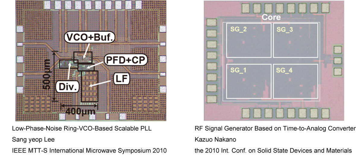 In high frequency integrated circuits for communication, CMOS has high performance in accordance with technology scaling, but its operating voltage decreases with scaling. This is due to the reduced drain breakdown voltage and dielectric breakdown voltage, but this low voltage operation that determines the consumption power from power charging and discharging of the load capacity shows a positive effect in the digital CMOS integrated circuit. However, in analog circuit, it is directly linked to the difficulty to secure the dynamic range.
Previously, passive components such as inductors and capacitors have been used in narrowband circuit, and the size of these components are determined by frequency used, therefore size of analog circuit on CMOS chip is very much affected. nH order inductor usually need more than 100μm square, but by using advance CMOS process and embedded processor, 200μm square inductor can be achieved. Since digital circuit cannot be mounted below the inductor, it consumes a comparatively large area on chip. Thus, passive components cannot be reduced in area in accordance with CMOS technology scaling in RF CMOS integrated circuit, and as a result we face a problem where it has no advantage in cost reduction benefits in miniaturization. Furthermore, reconfigurable circuit technique to accommodate cognitive communication technology has become necessary to support multiple wireless standards.
In this study, we are developing circuit technique which only consists of MOSFET (active component), and yet, it is a wideband operational Scalable RF CMOS circuit. ‘Scalable’ here means as the utilized CMOS technology generation progressed, the circuit also shows improvement in size consumption, as well as its performance. One of RF CMOS circuit direction is SoC with digital circuit. In effort to SoC, it is important to secure the scalability in analog CMOS circuit and RF CMOS circuit.
In high frequency integrated circuits for communication, CMOS has high performance in accordance with technology scaling, but its operating voltage decreases with scaling. This is due to the reduced drain breakdown voltage and dielectric breakdown voltage, but this low voltage operation that determines the consumption power from power charging and discharging of the load capacity shows a positive effect in the digital CMOS integrated circuit. However, in analog circuit, it is directly linked to the difficulty to secure the dynamic range.
Previously, passive components such as inductors and capacitors have been used in narrowband circuit, and the size of these components are determined by frequency used, therefore size of analog circuit on CMOS chip is very much affected. nH order inductor usually need more than 100μm square, but by using advance CMOS process and embedded processor, 200μm square inductor can be achieved. Since digital circuit cannot be mounted below the inductor, it consumes a comparatively large area on chip. Thus, passive components cannot be reduced in area in accordance with CMOS technology scaling in RF CMOS integrated circuit, and as a result we face a problem where it has no advantage in cost reduction benefits in miniaturization. Furthermore, reconfigurable circuit technique to accommodate cognitive communication technology has become necessary to support multiple wireless standards.
In this study, we are developing circuit technique which only consists of MOSFET (active component), and yet, it is a wideband operational Scalable RF CMOS circuit. ‘Scalable’ here means as the utilized CMOS technology generation progressed, the circuit also shows improvement in size consumption, as well as its performance. One of RF CMOS circuit direction is SoC with digital circuit. In effort to SoC, it is important to secure the scalability in analog CMOS circuit and RF CMOS circuit.
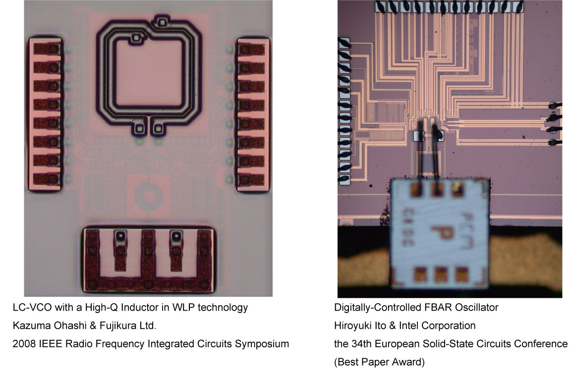 Besides, it is said that the only successful business in integrated circuit up until now is in the mass production of small kind of memory and MPU. The fact that miniaturization of integrated circuit are facing many challenges means that there is a change of perspective on the direction of development which is good. Disruptive innovation suggests an interesting idea. Instead of following the high-end market demand, “drop performance” and try to develop a new low-end market is a theory that proves that actually a sustainable technology can destroy high-end market imperceptibly. As an engineer, “dropping performance” is an uncomfortable part of it, but in CMOS technology development, rather than using advance CMOS, trying to practically use mature CMOS technology and this disruptive innovation might be able to produce integration with diverse functionalities. Integrations such as of MEMS and CMOS, CMOS and packaging technologies are considered to be an interesting exit. “MEMS-Enhanced RF Circuit” group is doing research development and aims to improve RF circuit performance by using MEMS technology significantly.
High speed transmission technology
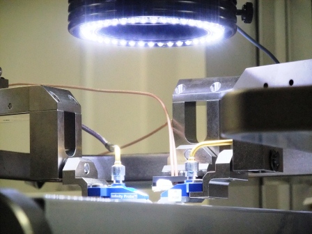
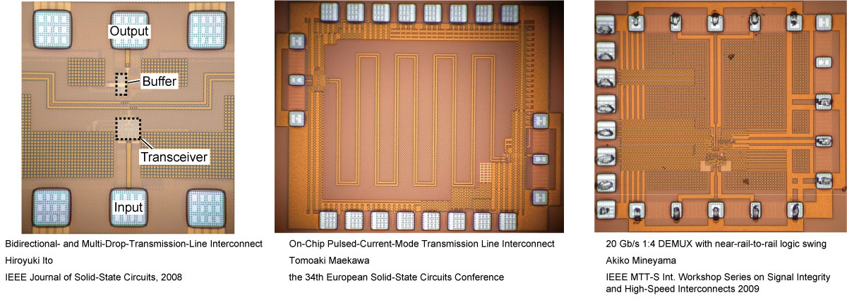
Keyword(s): On-chip transmission line, High efficiency signal transmission, High frequency measurement technology, De-embedding technique (up to 110GHz) |
|---|
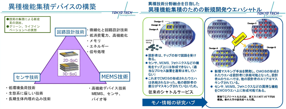
Multifunctional platform・interface technology
Keyword(s):Microelectromechanical System (MEMS), Fushion technique,Shuttle service |
|---|
Green ICE Initiative Project
To sustain development of society and industry as well as avoid global warming, we need to find way for Green (low calorie consumption, low environmental impact), Dependable (high performance, high reliability, high safety), ECO (eco-friendly) society Neural Networks (Information Network System) and social vascular network (the energy network system, transportation system). Through this, advancement and high reliability of the society and the whole industry is aimed to be well-balanced with energy-saving, CO2 control and ECO. We breakthrough the obstructed economic situation to create a sustainable advanced information and energy-oriented society, and with joint effort between industry and academia, we try to achieve significant research findings that will contribute to new industries. |
|---|
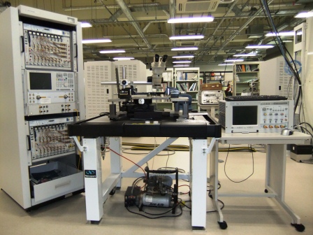
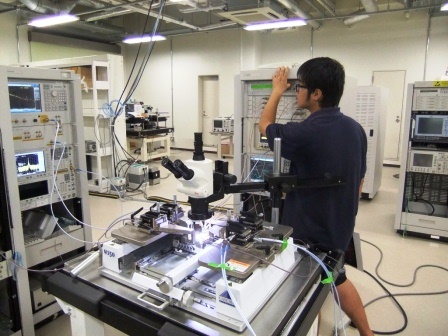
Experimental equipment
● Network analyzer |
|---|